Table of Contents
Parallella
bcrypt on Epiphany
This is a short description of bcrypt port on Parallella board, Epiphany Multicore Accelerator. First step was to make bcrypt work on one Epiphany core and after it make use of all 16 cores. When working implementation was obtained it was integrated with JtR.
One of encountered problems was host Epiphany communication. Compilers on Epiphany and on host side don't align variables on same boundaries. On Epiphany side variables are double-word aligned while on host they are single-word aligned. Because of that it is necessary to add dummy variables in shared buffer on host side to have same offsets on Epiphany and on host side.
Optimizations were done in assembly to make use of Epiphany dual-issue architecture. Some integer instructions are moved to FPU which is used in integer mode so that FPU instructions can be issued in parallel with other IALU instructions. Optimization is limited because FPU is capable of issuing addition and multiplication integer instructions while logical and load/store instructions can be executed only on IALU.
bcrypt on ZedBoard
This section contains description of bcrypt on ZedBoard implementation and instructions for creating bitstream and using FPGA resources on Parallella board for bcrypt format. PlanAhead project can be downloaded here
Bcrypt most costly loop is implemented on FPGA while other computation is done on host. Host and FPGA communicate using shared block RAM. Communication scheme is based on AR# 50826 and on this forum thread. In order to use block RAM, bcrypt IP has BRAM controller interface which is connected to shared BRAM. Because of this, only one BRAM port is used during computation which is big performance penalty. One of optimization steps will be copying S-box from shared BRAM to true dual-port BRAM which will be used during computation.
Parallella Platform bitstream
The first step is to follow Parallella Platform Reference Design and create Parallella platform bitstream. After creating Parallella platform bitstream it is necessary to change files provided on SD card and build Linux so that bitstream created in the previous step can be used on the system. This has to be done because original SD card image has support for other peripherals (such as HDMI) which are missing in HDL files used in Parallella Platform Reference Design. Replacing bitstream without modifying SD card contents causes Linux to crash. Before compiling device tree, this patch needs to be applied.
Adding bcrypt to Parallella Platform
Open general settings in Xilinx Platform Studio. Check Enable M_AXI_GP0 interface under General Purpose Master AXI Interfaces. Under High Performance Slave AXI Interfaces check Enable S_AXI_HP0 interface. Under Accelerator Coherency Port (ACP) Slave AXI Interface check Enable S_AXI_ACP interface and Enable ACP access for HIGHOCM address range. All other options should remain unchanged.
Next step is to add DMA, block RAM and bcrypt IP to the system module. AXI Central DMA can be found in IP catalog under DMA and Timer, add it to design. Click Yes on Add IP Instance to Design box. Window with options will open, don't change anything and click OK. Window Instantiate and Connect IP opens, choose User will make necessary connections and settings and click OK.
Find AXI BRAM Controller in IP catalog under Memory and Memory Controller and add it to design. In options window check Slave Single Port BRAM under AXI, leave everything else unchanged and click OK. Choose User will make necessary connections and settings and click OK. Add Block RAM (BRAM) Block to design.
Open /path-to-your-project/project_name.srcs/sources_1/edk/system/pcores and copy bcrypt_v1_00_a directory in opened folder. In XPS click on Project→Rescan User Repositories. In IP catalog, Project Local PCores will appear with bcrypt IP. Add BCRYPT to design.
Under Bus and bridge find AXI Interconnect IP and add 3 instances to design (without changing anything).
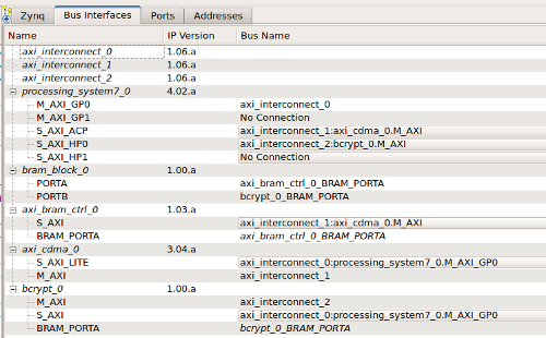
Next step is to connect added IPs. Under Bus Interfaces tab expand processing_system7_0. Connect M_AXI_GP0 to axi_interconnect_0. Expand axi_cdma_0 and connect M_AXI to axi_interconnect_1. Connect S_AXI_LITE to axi_interconnect_0:processing_system7_0.M_AXI_GP0. Expand axi_bram_ctrl_0 and connect S_AXI to axi_interconnect_1:axi_cdma_0.M_AXI. Expand bram_block_0 and connect PORTA to axi_bram_ctrl_0_BRAM_PORTA. Connect PORTB to bcrypt_0_BRAM_PORTA. Expand bcrypt_0 and connect M_AXI to axi_interconnect_2 and S_AXI to axi_interconnect_0:processing_system7_0.M_AXI_GP0. Expand processing_system7_0 and connect S_AXI_ACP to axi_interconnect_1:axi_cdma_0.M_AXI and S_AXI_HP0 to axi_interconnect_2:bcrypt_0.M_AXI.
Under Port tab expand axi_interconnect_0, 1 and 2. Connect INTERCONNECT_ACLK to processing_system7_0::FCLK_CLK0 and INTERCONNECT_ARESETN to processing_system7_0::FCLK_RESET0_N. Expand axi_bram_ctrl_0, axi_cdma_0 and bcrypt_0 and connect (BUS IF) clock ports to processing_system7_0::FCLK_CLK0.
Expand processing_system7_0. Make sure that FCLK_CLK0 has connection External Ports::processing_system7_0_FCLK_CLK0_pin. Connect (BUS IF) M_AXI_GP0, (BUS IF) S_AXI_HP0 and (BUS IF) S_AXI_ACP clock to processing_system7_0::FCLK_CLK0.
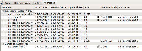
Under Addresses tab click on Generate Addresses button. Expand processing_system7_0. Set size of axi_cdma_0 and bcrypt_0 to 8K. Set axi_cdma_0 C_BASEADDR to 0x40000000 and bcrypt_0 C_BASEADDR to 0x40002000. Click Generate Addresses button one more time. Expand Unmapped Addresses and set size of axi_bram_ctrl_0 to 8K and it's C_BASEADDR to 0x40004000.
Run design rule check. Close XPS and in PlanAhead window click on Generate Bitstream.
Replacing bitstream on Parallella platform
Bitstream file can be replaced using the Linux driver for DEVCFG. AR# 46913 suggests using BootGen tool for converting bitstream to a binary but using promgen tool is much simpler because it does not require First Stage Boot Loader and U-boot.elf file. Bitstream can be converted to a binary using following command:
promgen -b -w -p bin -data_width 32 -u 0 top_parallella16_prototype.bit -o top_parallella16_prototype.bit.bin


