Table of Contents
Implementation of Bcrypt algorithm in hardware (GSoC 2011 qualification task - archived, obsolete)
This wiki page contains archived and obsolete content from GSoC 2011. For up to date information on bcrypt on FPGA, please refer to the parent page.
This is part of a qualification task regarding the GSoC 2011 proposal of Yuri Gonzaga Gonçalves da Costa.
I) High level implementation
First of all, the algorithm was coded in Java. This step was important to understand the algorithm in details in order to implement it in hardware later.
II) High level testing
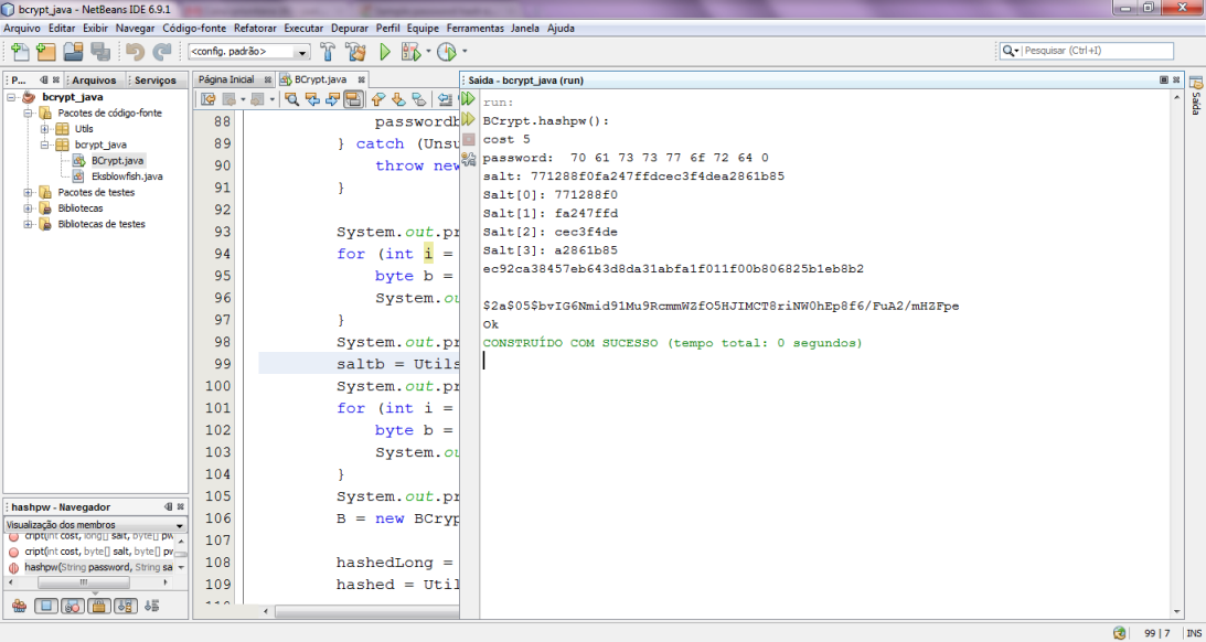
Some test cases were employed to validate this functionality. Below, it is presented a screenshot (using NetBeans IDE) of a test case as proposed in http://openwall.info/wiki/john/sample-hashes. The file BCrypt.java in the Java code uploaded has a Main method that implements this test case.
III) Hardware level implementation
It was implemented in SystemVerilog language (http://www.systemverilog.org/). A protocol based on Ready and Valid signals was used as handshake to read input data and write output data. Also, this module models a state machine to control the algorithm steps. All the S-boxes and P-array were implemented in registers as a first version. However, in the future, it will be replaced by memory ram blocks and save FPGA resources.
IV) Hardware level simulation
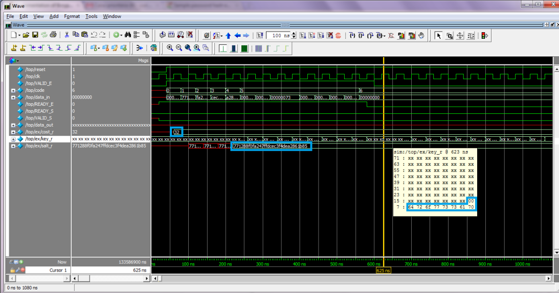
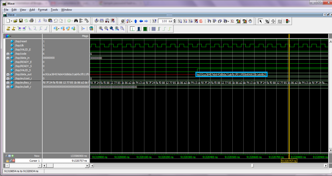
The MentorGraphic's Questasim tool was employed to simulate the SystemVerilog implementation. The same test cases of high level testing were used to verify its functionality. This way, it is possible to compare the high and low level results. Two screenshots of waveforms is provided to show one example of hardware simulation (the same showed above in high level testing). In the SystemVerilog code uploaded, the file top.sv implements this test case.
The highlighted values point the contents of inputs cost, salt and key. Note that cost stores the result of power of 2 (in this case, 2ˆ5 = 32). The result is outputed after 91320350 ns. Considering a clock frequency of 25 MHz (period of 40 ns), the number of clock cycles wasted to calculate the hash is 2283008.
V) FPGA synthesis results
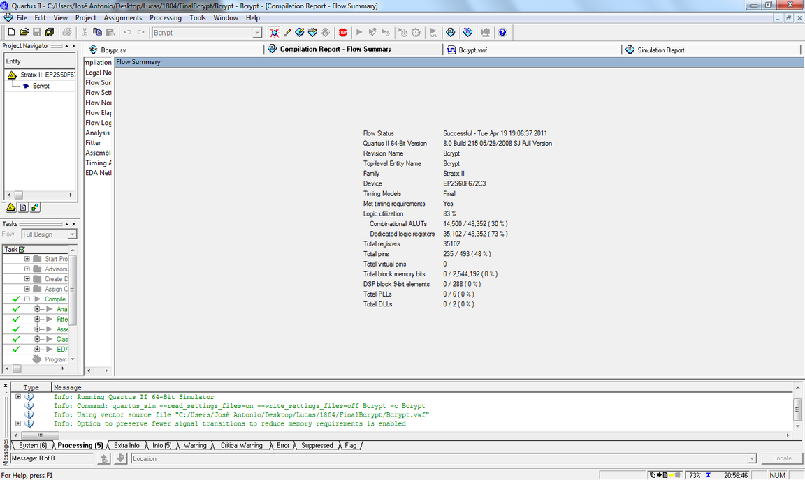
Bcrypt module was synthesized to Altera's EP2S60F672C3 FPGA device (Family Stratix II) using Quartus II v. 10.0 software. Results show that it is using 14,500 combinational ALUTs and 35,102 dedicated logic registers. Those values correspond to 83% of resources usages. Once memory blocks will be used in the future, this should decrease greatly in next versions. The maximum frequency achieved is 96 MHz (period of 10.4 ns). Considering this clock frequency in the above example, the time to hash that key is about 23 miliseconds.
VI) FPGA board communication
I am trying to use JTAG interface provided in Altera's Nios Development Board - Stratix II Edition - to communicate the hardware system to JtR through USB-Blaster Cable also provided in this kit. However, it is not yet working well.
VII) JtR integration
The JTAG interface is accesible by software through Tcl scripting interpreted by quartus_stp program. The idea is to generate a script and call quartus_stp program in execution time of JtR to pass input data to hardware and receive result back. By now, it is only a idea because nothing was done yet.
John the Ripper 1.7.8 modified for easy integration of multiple Eksblowfish cores (by Solar Designer)


